Enabling Hidden UART Debug on Nintendo Switch 1 Docks
Introduction
While trying to repair a broken original Nintendo Switch (HAC-007) dock, I discovered that the STM32 MCU on the board has a hidden UART debug output, disabled in firmware by a single flag. A one-byte patch re-enables it. This is a quick write-up on how I found it and how to turn it on, in case it’s useful for anyone else repairing these docks.
The Hardware
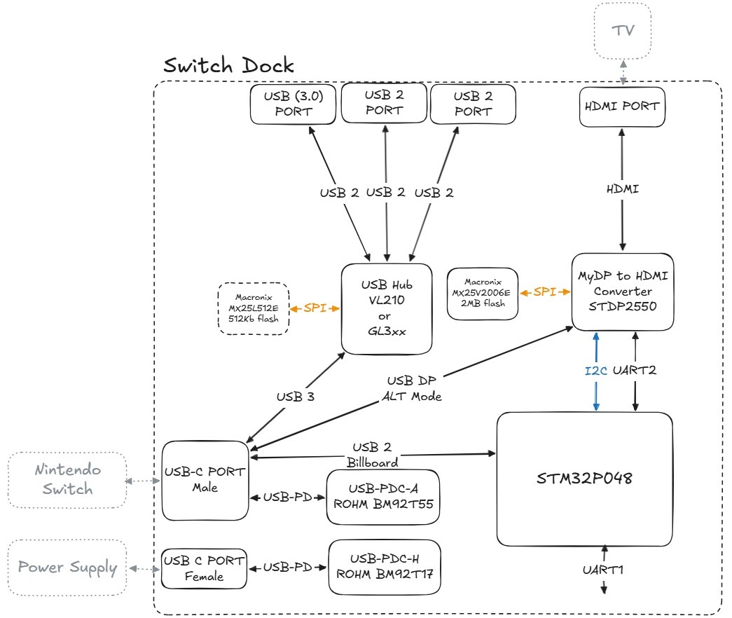
Block diagram of the Nintendo Switch 1 Dock (HAC-007).
The original Switch 1 dock is essentially a USB-C multifunction adapter that combines power negotiation, USB expansion, and video conversion. A USB-C PD controller negotiates power from the external charger and presents the correct dock power profile to the Switch, while the Switch’s USB link feeds an internal USB hub that fans out to the dock’s USB-A ports (with a small SPI flash often used for hub configuration). For TV output, the Switch switches its USB-C connection into DisplayPort Alt Mode, sending DP lanes into a DP-to-HDMI converter (STDP2550) that drives the HDMI port, typically backed by its own SPI flash for firmware and configuration. An STM32 microcontroller ties it all together by sequencing and monitoring the system, talking to the video converter over I²C and handling attach/detach and control logic.
USART1 of the STM32 seems to be the debug port for the MCU, and USART2 seems to be connected to the STDP2550, although I was never able to get any output from it. Interestingly, the readout protection on the STM32 is not enabled, so we can just read out the firmware and patch it to enable the debug output.
Luckily UART1 on the PCB is easily accessible on a testpoint.
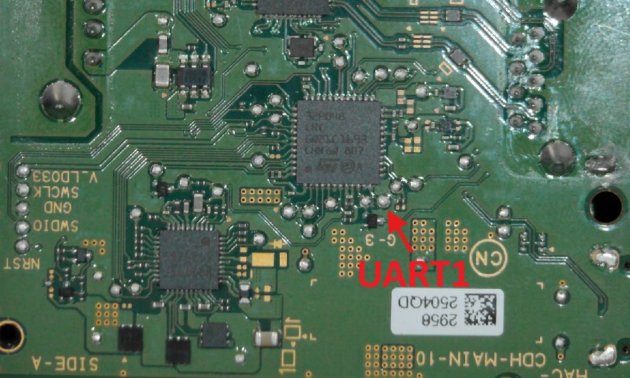
UART1 Testpoint on the PCB.
Examining the Firmware
Usually with reverse engineering tasks I first let AI have a go at it and see if it can give me some initial insights. This time I took a more hands-on approach, since I’m fairly familiar with Cortex-M firmware and reverse engineering it in Ghidra. So I loaded up the firmware dump and my first stop was the string table.
 BC Config
 BC Interface
 Nintendo
 CRD-001
 16/1/1
--1--
--2--
--3--
--4--
 TEST_USER_STR_DESC
/F.F
O*F9F
CALLSETUP
GET_DESC
BOS_DESC
PPEMP
FFpG
!F(F
pJxBp
2QapG
)F F
Nov 11 2016
09:30:01
...
There I found some interesting strings, and some of them looked like debug messages. But I wasn’t recognizing any output on the UART. Checking the cross-references for these strings led me to a function that looks like some kind of print function.
int print(char *__format,...)

{
  char cVar1;
  undefined2 uVar2;
  uint uVar3;
  uint uVar4;
  int iVar5;
  int iVar6;
  undefined4 in_r1;
  undefined4 uVar7;
  uint uVar8;

  uVar3 = strlen();
  iVar6 = DAT_0800028c;
  uVar3 = uVar3 & 0xff;
  if (((uVar3 == 0) || (0x1e < uVar3)) || (*(char *)(DAT_08000288 + 1) == '\0')) {
    return 1;
  }
  uVar4 = 0;
  uVar7 = 0;
  uVar8 = 0xff;
  do {
    if (uVar3 <= uVar4) {
      for (uVar8 = 0; uVar8 < uVar3 + 1; uVar8 = uVar8 + 1 & 0xff) {
        *(char *)(iVar6 + uVar8) = __format[uVar8];
      }
      goto LAB_0800026c;
    }
    if (__format[uVar4] == '%') {
      cVar1 = __format[uVar4 + 1];
      if ((cVar1 == 'x') || (cVar1 == 'X')) {
        uVar7 = 0x10;
        uVar8 = uVar4;
      }
      else if (cVar1 == 'd') {
        uVar7 = 10;
        uVar8 = uVar4;
      }
    }
    uVar4 = uVar4 + 1 & 0xff;
  } while (uVar8 == 0xff);
  for (uVar4 = 0; uVar4 < uVar8; uVar4 = uVar4 + 1 & 0xff) {
    *(char *)(iVar6 + uVar4) = __format[uVar4];
  }
  iVar5 = FUN_08001e88(in_r1,uVar7,iVar6 + uVar8);
  for (uVar8 = uVar8 + 2; uVar8 = uVar8 & 0xff, uVar8 < uVar3 + 1; uVar8 = uVar8 + 1) {
    *(char *)(uVar8 + iVar5 + iVar6 + -2) = __format[uVar8];
  }
LAB_0800026c:
  uVar2 = strlen(DAT_0800028c);
  iVar6 = FUN_08003ee0(DAT_0800028c + 0xa4,DAT_0800028c,uVar2,100);
  if (iVar6 != 0) {
    return 1;
  }
  return 0;
}
I noticed that print was checking a flag at *(char *)(DAT_08000288 + 1) before it would actually output anything. Following where this flag was set led me to the initialization code, where it was being set to 0, meaning debug output is disabled by default. This is likely a flag that would only be set for debug builds during development.
Enabling the Debug Output on UART1
To permanently enable debug output, we just need to patch the print function to skip the gating check:
| Address | Original | Patched | Effect |
|---|---|---|---|
0x080001EA |
4B D0 (beq LAB_08000284) |
00 00 (NOP) |
Skip the gating check |
This replaces the conditional branch with NOPs, so print never returns early.
After flashing the patched firmware, powering on the dock greets us with the following UART output:
Nov 11 2016\r\n
09:30:01\r\n
3-01\r\n
And when connecting a Switch:
3-B3\r\n
4-01\r\n
When we disconnect the Switch, we get:
3-01\r\n
Interpreting the UART1 Output
Interpreting these strings was the hard part. While I could compare output between a working and a broken unit, I wanted to get more context about what each code actually means. Especially the codes related to the HDMI/video output state machine. I have no prior knowledge of how DP-to-HDMI conversion is sequenced, and manually reverse engineering the meaning of each debug string would have taken significantly more effort than the patch itself.
This part was almost completely handled by GitHub Copilot with Claude Opus 4.5, which I gave access to the firmware binary and some Linux tools. After some back-and-forth, I came up with the following interpretation of the debug strings. Since these were largely produced by an LLM, take them with a grain of salt … I’m not sure all of them are correct, but they seem to make sense. The format appears to be X-YY, where the first digit indicates which state machine is reporting and the second part is the actual state within it.
| Code | State machine | Meaning |
|---|---|---|
3-01 |
hdmi_bring_up_machine | Initialized / undocked |
3-B3 |
hdmi_bring_up_machine | Switch connects |
3-W1 |
hdmi_bring_up_machine | |
4-01 |
pwr_link_machine | Connection Initialized - Video should be active |
5-01 |
dp_video_machine | |
5-B1 |
dp_video_machine | |
5-W1 |
dp_video_machine | |
HNCES->FErr |
Error ? | |
FATAL X-Y |
System failure with additional error codes |
A Brief Look at the STDP2550
Running the strings command on the STDP2550 firmware dump reveals a lot more interesting debug strings and hints that there is a command handler implemented:
wrong param input
+++Lane number OOR. Setting to 0.
#Bathtub curve for Lane %d with PRBS7
#Bathtub curve for Lane %d with Video Stream
#AdjReg=0x%x /EQ=0x%x/FP=0x%x/CP=0x%x /DR=0x%x
##FP= 0x%x
##EQ=0x%x
+++Error count is invalid
END$$$$$$$$$$$$$$$$$$$$$$$
0 - Appstest Desc [<Param0>] [<Param1>] [<Param2>] [<Param3>]
5 - DPRX Intenal Test Pattern
     - Param0: H Active
     - Param1: V Active
     - Param2: V Freq
6 - Enable DP Lib Debug Prints
     - Param0: 1: Enable, 0:Disable
7 - Prints pre-fetched EDID location in RAM
8 - Disable DPRX Intenal Test Pattern
9 - FW version
31 - Host Interface Read
   - Param0: host interface address (ex.0x0)
32 - Host Interface Write
   - Param0: host interface address (ex.0x0)
   - Param1: value in word (ex. 0x1234)
   - Param2: if invoking action function (0: FALSE,1:TRUE)
41 - HDMI TX PBus Write
    - Param0: address (16 bit)
...
However, I was never able to get any output from its UART pins. The datasheet suggests it runs some 16-bit CPU core, and only later versions of this chip family started using Cortex-M cores. Given that, I wasn’t interested in doing a full reverse engineering effort on this firmware.
Fixing My Switch Dock
In my particular case, the debug output was unfortunately not too helpful. It hinted that the STDP2550 should be working, but it wasn’t. After more investigation, it turned out that some I/O cells of the STDP2550 were damaged and the chip was no longer able to drive the HDMI signal. I had to source a replacement chip and swap it out to get the dock working again. But at least now I know the debug output is there and could be helpful for other types of repairs.
Conclusion
So there it is: a hidden debug UART port on the Switch 1 dock, disabled in firmware with a simple flag check. It’s a one-byte patch to re-enable it. Not sure why they felt the need to disable it in production. It could genuinely help during repairs. Although I have to admit that in my particular case, and in many of the common dock failure modes, this alone wouldn’t have pointed me to the root cause.
What I found more interesting was how much LLMs accelerated the reverse engineering process. For the firmware analysis and interpreting the debug codes, I mostly just had to supervise. I think without that, I probably wouldn’t have dug as deep into this particular project. It’s becoming a useful tool in the hardware hacker’s workflow, especially for the tedious parts of firmware RE.